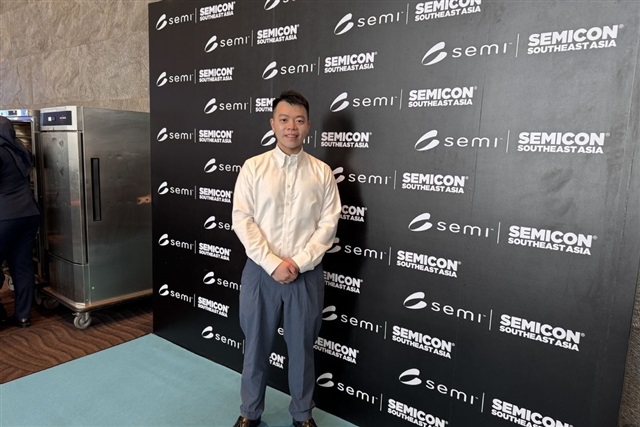
Galatek, a Singapore-based AI automation startup, is tackling yield bottlenecks in micron-level adva...
The AMW Read
Incremental update: a new entrant in AI-for-semiconductor-manufacturing subsegment; no disclosed funding or product release to move beyond baseline novelty. Sub-segment impact only.

Galatek, a Singapore-based AI automation startup, is tackling yield bottlenecks in micron-level advanced semiconductor packaging with AI-embedded equipment, according to Digitimes. The company is targeting Taiwan's foundry ecosystem as demand for AI and HPC chips surges across Southeast Asia and global markets. The article behind the paywall details the company's focus on packaging, a critical step in chip production where defects become disproportionately costly at advanced nodes.
Why it matters: Galatek's entry into advanced packaging intersects two structural forces in our substrate. First, it rides the "context-engineering moat" pattern — but applied to physical manufacturing rather than software. By embedding AI directly into packaging equipment, the startup aims to solve yield problems that grow exponentially with chip complexity, a bottleneck that hyperscaler-distribution dynamics (Section 3.PC) have not yet addressed. Second, it underscores the Southeast Asian semiconductor push, where Singapore is positioning itself as a packaging hub amid US-China decoupling — a geopolitical force (Section E) that reshapes supply chains. This is not a capital-cycle story (no funding disclosed) but a technology-expansion move that updates the player map for AI in semiconductor manufacturing.
Expert take: Galatek is betting that the next frontier for AI in hardware is not just chip design or EDA, but the physical process of packaging — an area historically dominated by tool providers like ASMPT and Applied Materials. If successful, AI-embeded equipment could become a new category in the semiconductor supply chain, potentially creating acqui-licensing targets for larger equipment makers. The Taiwan foundry focus is strategic: TSMC's advanced packaging capacity is a key bottleneck for AI accelerators, and any yield improvement there directly benefits the entire AI compute substrate. This is a nascent but real signal of AI moving deeper into semiconductor manufacturing's operational layer.
#AdvancedPackaging #AIinSemiconductors #Galatek #SemiconductorManufacturing #SingaporeTech #YieldOptimization