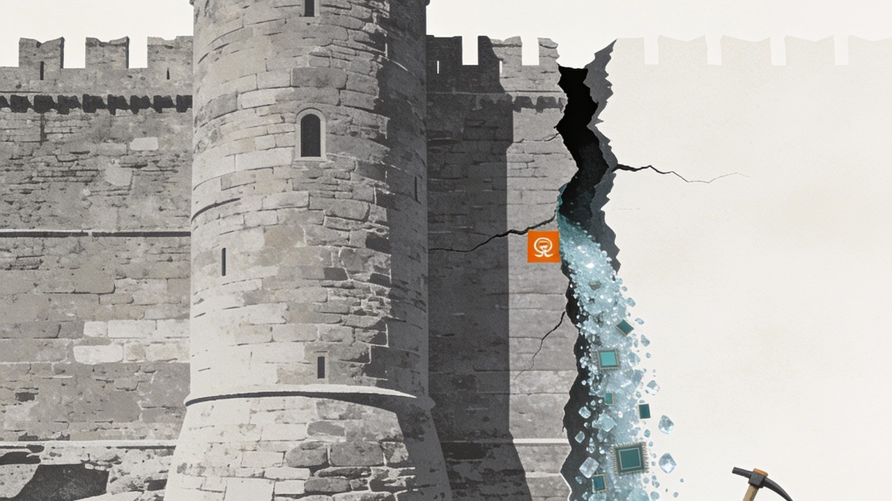
The Great Silicon Decoupling: Inference Chips Flood the NVIDIA Moat
Etched, a startup founded by three Harvard dropouts, secured a $1 billion chip order for its Sohu ASIC while raising $800 million at a $5 billion valuation—backed by Geoffrey Hinton, Fei-Fei Li, Andrej Karpathy, Peter Thiel, and a TSMC-affiliated fund Etched announcement. The chip is a 4nm ASIC designed exclusively for Transformer inference, and the company claims that an 8-card Sohu server can replace 160 NVIDIA H100s for Llama 70B, delivering 20x throughput and 140x cost-per-dollar improvement over GPU-based solutions. That single pre-production order—the strongest market validation yet for a dedicated inference chip—marks the moment the NVIDIA monopoly began to crack.
The scale of the shift is not isolated to one company. SambaNova Systems raised $1 billion in a Series F round led by General Atlantic, reaching an $11 billion valuation—a fivefold increase from its $2.2 billion valuation just five months earlier SambaNova funding. The company’s SN40L and SN50 inference chips claim 5-10x decode performance over NVIDIA GPUs for large language models, and JPMorgan Chase has deployed the systems for on-premises inference of sensitive financial data. FuriosaAI, Nuvacore, and D-Matrix are also raising new rounds as venture capital interest in AI hardware surges, driven by hyperscaler and enterprise demand for GPU alternatives chip funding spree. The collective capital inflow—over $3 billion across these three deals alone—signals that the market is voting for a multi-vendor inference silicon future.
The mechanism powering this decoupling is straightforward: general-purpose GPUs waste enormous energy on non-compute data movement. Etched’s Sohu achieves its advantage by hardwiring attention mechanisms into fixed silicon, reaching 80–90% peak FLOP utilization versus ~40% on H100 Etched benchmark analysis. But the advantage is not uniform—at batch-1, Sohu’s throughput advantage over H100 collapses to roughly 1.4x because memory bandwidth becomes the bottleneck, not compute. The 20x claim applies to high-batch-size, short-context workloads where weight reuse is maximized. No Sohu hardware has shipped to production customers, and no independent benchmarks exist under production conditions. The ASIC’s fixed-hardware assumption also carries architectural risk: if future model architectures shift from Transformers to state-space models or hybrid attention, the chip’s hardwired attention mechanisms become stranded assets.
Meanwhile, a different path to inference efficiency is emerging from the memory layer. SK Hynix, the world’s second-largest memory maker, partnered with US startup tetraMem to validate a memristor-based in-memory computing SoC that achieves 21.3 TOPS/W at 100MHz on a mature 65nm CMOS process—matching a 4-bit quantized software baseline SK Hynix tetraMem validation. This efficiency figure is an order of magnitude better than NVIDIA’s A100 INT8 performance, which typically achieves ~0.5–2 TOPS/W Tom's Hardware comparison. The test chip is lightweight—only 2.54 TOPS peak throughput—but it demonstrates that analog in-memory computing on older, cheaper nodes can achieve 21.3 TOPS/W, compared to 0.5–2 TOPS/W for digital accelerators. For edge AI and power-constrained inference, this could reshape the economics entirely, reducing hyperscaler dependence on leading-edge foundry capacity.
The decoupling is not confined to data centers. NVIDIA itself demonstrated the RTX Spark superchip in production laptops at Bilibili World, packaging a Blackwell GPU with a 20-core Grace CPU via NVLink-C2C, sharing 128GB of unified memory and delivering 1 Petaflop of compute RTX Spark demo. The chip runs 120B-parameter models locally at up to 1 million tokens of context length. NVIDIA is taking its own data-center architecture and shrinking it into a personal form factor—a defensive move that acknowledges that inference silicon is becoming a distributed, multi-form-factor market. Apple’s M7 Ultra chip, accelerated with up to 1.5TB RAM and Neural Engine upgrades derived from the abandoned self-driving car project, will serve as the basis for a new Apple server product expected in the first half of 2027 Apple M7 Ultra. But Apple plans to use the M7 Ultra exclusively for its own Apple Intelligence cloud infrastructure, not for resale—meaning it will not compete directly with NVIDIA or AMD in the general server market TechTimes analysis. The lesson is that even the most vertically integrated player is building its own inference silicon to escape the NVIDIA tax.
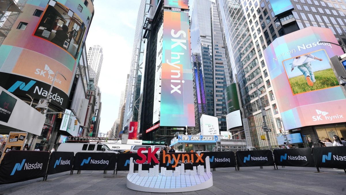
The precedent for this fragmentation is visible in the memory supply chain. SK Hynix raised $26.5 billion in the largest foreign IPO in US history, eclipsing Alibaba’s 2014 record, to fund HBM capacity expansion SK Hynix IPO. The IPO crystallizes the capital-compression arc: investors now price AI memory assets based on their hyperscaler distribution moat, not legacy geography discounts. Simultaneously, SK Hynix is exploring post-HBM architectures through the tetraMem partnership, signaling that the memory giant sees in-memory computing as a credible successor technology SK Hynix tetraMem validation. The combination of HBM-scale capital and IMC research suggests that the memory-compute boundary is dissolving, and the next generation of inference silicon may not look like a GPU at all.

The ripple effects are already visible in the middleware layer. Model routers—intelligent middleware that dispatches queries to cheaper or smaller models, reserving frontier APIs only for complex requests—are gaining adoption as enterprises face escalating inference costs model routers. Early adopters report cutting inference spend by 30-50% without sacrificing output quality. This creates a new layer of inference arbitrage: when the router learns which model performs best on which query, the cost of switching between silicon providers drops to near-zero. SiliconFlow, China’s largest independent AI token supply platform, filed for a Hong Kong IPO at a $1.07 billion valuation, despite negative gross margins of -24% as it spent heavily on compute procurement and free-token marketing SiliconFlow IPO. The company’s 653% revenue growth in 2025 illustrates the “fastest-ARR-ramp” pattern, but its negative unit economics also show the brutal margin compression that inference infrastructure faces when competing with hyperscaler-owned platforms.
The implication for enterprise buyers is both liberating and bewildering. Netrasemi, a Kerala-based startup, launched the A2000 edge AI chip on TSMC’s 12nm process, targeting smart cameras and video gateways, with plans for mass production in 2027 Netrasemi A2000. Yunbao Intelligent, a Tencent-backed DPU startup, filed for a ChiNext IPO in Shenzhen with 2025 revenue of $510 million, aiming to become China’s first publicly traded DPU company Yunbao IPO. The silicon landscape is fragmenting into specialized niches: Transformer ASICs, memristor-based IMC, edge AI accelerators, DPUs, and personal superchips. Enterprises now face a procurement landscape that requires evaluating not just performance and price, but architectural compatibility, software ecosystem maturity, and supply chain resilience.
The great decoupling is real, but it is not a clean victory for any single alternative. Etched’s Sohu claims a 20x throughput advantage over H100 only at high batch sizes with short contexts; at batch-1 the advantage is roughly 1.4x, and no production benchmarks exist Etched benchmark analysis. SambaNova’s 5x valuation surge in five months reflects investor hunger for NVIDIA alternatives, but the company has not disclosed production-scale deployment metrics. The memristor chip from SK Hynix and tetraMem is a research validation, not a commercial product. NVIDIA’s RTX Spark and Apple’s M7 Ultra show that the incumbent and the platform player are also racing to own the inference layer. The market is not switching from NVIDIA to a single winner; it is transitioning from a single-vendor GPU monopoly to a multi-form-factor, multi-architecture inference market where NVIDIA remains the largest player but no longer the only viable option.

This fragmentation is the structural opportunity and the risk. It gives enterprises the ability to negotiate, to mix and match silicon for different workloads, and to build private infrastructure that bypasses the hyperscaler distribution tax. But it also introduces complexity: evaluating ASIC longevity against model architecture shifts, managing software stacks that are not CUDA-compatible, and navigating supply chains that are increasingly geopolitical. The decoupling is underway, and the winners will be those who can navigate the fragmentation, not those who bet on a single successor to the GPU.
